
Semiconductor Series, Part I : Raw Materials and Wafer Fabrication Equipment (WFE)
There are many different kinds of chips: wood chips, potato chips, poker chips etc. but perhaps the most important variety of chip is the computer microchip. These types of chips are a culmination of human scientific progress, and continue to push the boundaries of physics with every new generation. They act as the brains that power our everyday lives, from household items like smartphones and microwaves to the massive supercomputers that we use to predict the weather. Today, chips are not just a gadget that provides us with the personal convenience of Google, but they have evolved to become a topic worth discussing at a geopolitical and anthropological scale.
The semiconductor industry is one of the fastest developing and geopolitically important industries on earth. Understanding the semiconductor industry serves its purpose not only by satiating one’s own curiosity, but it also provides a new angle for evaluating the international relations between China, Taiwan, and the United States. This 3 part semiconductor series will be an industry overview of the semiconductor space, starting with Part I: Raw Materials and Equipment Manufacturers.
The most important raw material in the semiconductor industry is the semiconducting element itself, Silicon. This element can be doped with other elements, and then controlled using an electric field to determine its conductivity. Humans leveraged this quality of Silicon to build out logical circuits that can do all sorts of operations. The other element you’ll find abundantly in a chip is Copper. These make up the local roads, highways, interstates, freeways, and elevators that carry data around the chips. You also can’t forget about the Metal-Oxide based photoresists. This material acts as the paper in which chip designs are stenciled onto, and needs to be layered onto the same chip up to 100 separate times throughout the chipmaking process.
Let’s examine exactly how these materials are used in the process. Each computer chip originally started off as sand, silica sand to be specific. The silica sand will then be melted into molten silicon, then a small silicon crystal will be dipped into the molten silicon, acting as the base crystalline structure for the molten silicon to attach onto. In this way, a solid round silicon ingot is pulled from the molten liquid, and then sliced into half millimeter thick circular wafers. Each individual wafer is like a canvas, for tens if not hundreds of chips to be imprinted into. Here is a graphic of the chipmaking process made by Branch Education:
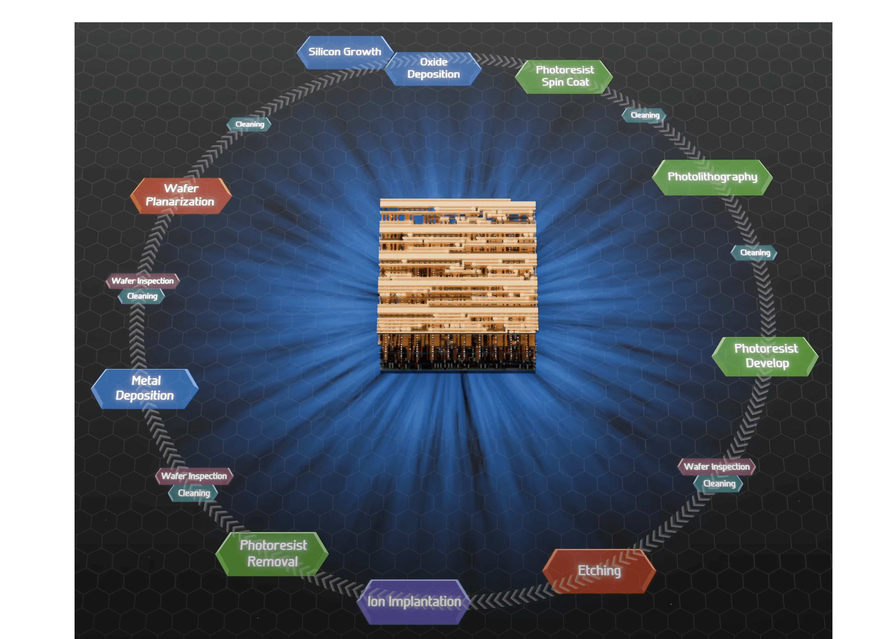
The first step in the process is doping the silicon. In order to do this, a layer of silicon dioxide is added to the entire wafer using a deposition machine likely made by Applied Materials. A photoresist is then added on top using a machine from Tokyo Electron. The Metal-Oxide based photoresist reacts with UV light, either strengthening or weakening depending on the specific material.
This photo-resist covered wafer is then put into a photolithography machine built by ASML. This machine essentially uses what is called a photomask to imprint a design onto the photoresist. It is merely using a stencil and UV light to print a design onto the photoresist, altering the properties of part of the photoresist in an intricate way.
After stenciling a design in, the weak part of the photoresist is then dissolved using a developer made by Tokyo Electron
The newly exposed base layer of silicon dioxide is etched away in the stenciled design by an etcher made by Lam Research, Tokyo Electron, or Applied Materials.
The now exposed raw silicon is doped through a process called ion implantation, where the silicon wafer is bombarded with either Boron, arsenic, phosphorus, and occasionally gallium. The ion implantation machine, made by Applied Materials, literally shoots these elements at the silicon wafer.
A deposition machine is then used to deposit a new layer of silicon into the crevices of the photoresist.
The photoresist is then fully removed, and we are left with a silicon wafer that has been doped in a certain pattern. A planarization machine will then smoothen out the surface of the wafer, ensuring its uniformity for when the next layer is added.
This initial process will repeat for about 10-20 layers, and will create all the transistors on the chip, finishing the FEOL-front-end of line- process for chipmaking.
After the initial 10-20 layers, it is now time to build the data highways in the BEOL-back-end of line- process. How can one part of the chip relay information to another? It has 3 options depending on where it needs to send data, a local, regional, and global road system. These road systems are built through a similar process. The wafer will receive a deposition of silicon dioxide, then a photomask, then it will be weakened by lithography, which will allow the developer to remove the weakened portions. This is where the process changes. The exposed parts of the silicon dioxide layer will still be etched away, but in its place, will be newly deposited copper traces. This process will continue for another 100+ layers, there are a ton of interconnects
Next steps for the industry, and where opportunity might lie ahead:
The semiconductor industry moves fast, and equipment that was cutting edge a few years ago, can seem archaic today. The next big move in the semiconductor industry from a raw material and equipment manufacturing standpoint is the shift away from FinFET to Gaa-FET, short for gate-all-around field effect transistor. Here is the visual difference:
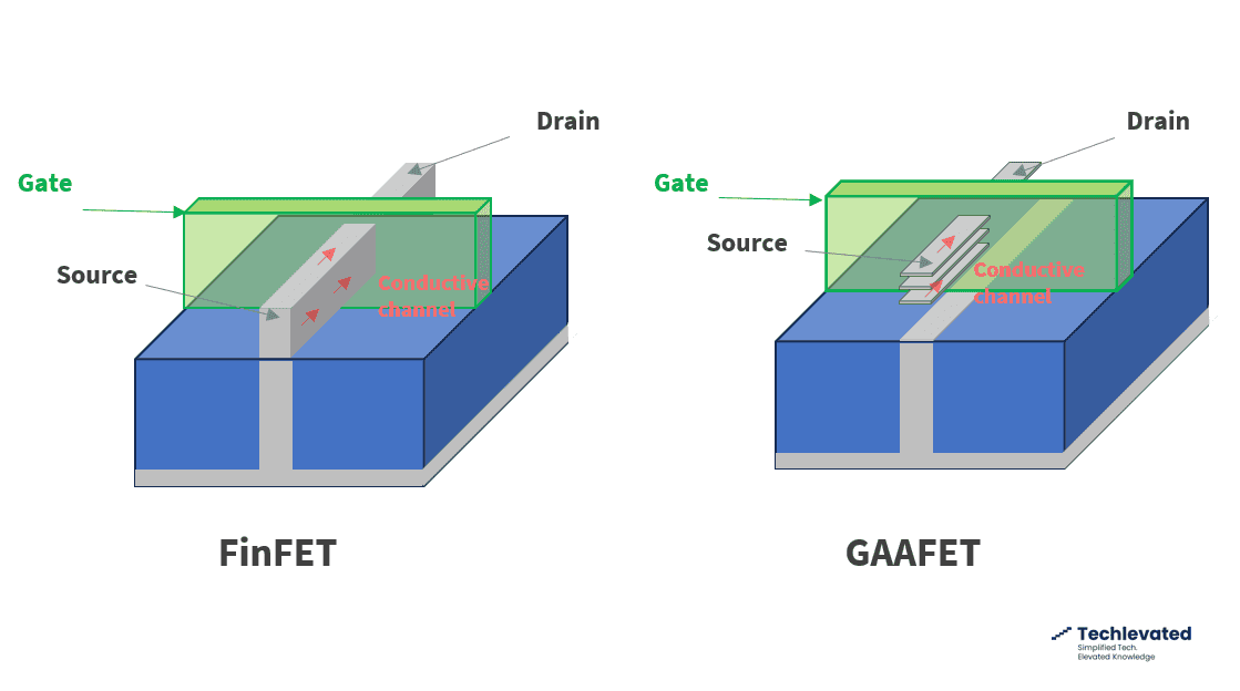
(Source: Techlevated)
Without going into the technicalities of why Gaa-FET is advantageous from a performance standpoint, one can just visibly see that Gaa-FET’s will require a more intricate build out along the vertical axis. For the same transistor, there now exists two more protruding fins in comparison to FinFET. These protruding fins are also oriented orthogonal with respect to the vertical axis, meaning that each fin necessitates its own layer, and by extension will pass through all those machines in the FEOL process another time. With additional layers, and more intricate transistors, the raw material suppliers that are likely to win are the photoresist and cleaning chemical suppliers. Each layer will require its own photoresist, and multiple rounds of cleaning. On the WFE side, the increase in layers is likely to be a rising tide for equipment manufacturers, as now there is more work to be done for the same chip. That being said, the one corner of the WFE market that should be poised to shine even brighter is metrology/inspection. FinFET was already quite intricate to manufacture, but Gaa-FET is a new beast all around. Put simply, we can use Murphy’s law, “Anything that can go wrong, will go wrong”. With the new structural complexity introduced by Gaa-FET, there will definitely be far more defects per unit area on the wafer. As such, metrology/inspection tools will take on an increasingly important role in the production line.
Who makes these machines, and how to get involved as an investor:
Now that you are familiar with the process, let’s examine the businesses behind each of these steps. To do this, we can try to piece together a case study for TSMC’s cutting edge fabs. The company gracefully provides a list of raw materials suppliers, so the only speculation will come from the WFE suppliers (Wafer Fabrication Equipment suppliers), which are concentrated around 5 big firms: ASML, Applied Materials, Lam Research, Tokyo Electron, and KLA-Tencor.
Starting off with the raw materials, we can see that for the raw silicon wafers, TSMC is supplied by:
F.K.S. (Formosa Komatsu Silicon)
SunEdison (Formerly Known as MEMC, Monsanto Electronic Materials Company)
Shin-Etsu Handotai
Siltronic
Sumco
TSMC lists their chemicals suppliers as:
BASF
Mitsubishi Chemical
These chemicals these companies supply TSMC are likely the cleaning chemicals like the pure ammonia water used to clean the wafers at each step.
TSMC’s photoresist suppliers are:
Merck (by way of AZ acquisition)
Shin-Etsu Chemical
Sumitomo
T.O.K. (Tokyo Ohka Kogyo)
TSMC’s gas suppliers are:
Air Liquide
Air Products
BOC (British Oxygen Company)
Taiyo Nippon Sanso
These gases are likely used in processes like the oxidation, vapor deposition, and vapor etching steps.
Among the raw material suppliers, Shin-Etsu Handotai is owned by Shin-Etsu chemical, so those count as one entity, and Sumco is a joint venture between Sumitomo and Mitsubishi.
As for WFE suppliers, we can only speculate as to whose equipment lines the cutting edge fabs of TSMC. Here is a quick graphic that represents the market share of each of the big 5 in each chipmaking process.

(Source: The China Project)
For the sake of our simplified model, let’s assume that TSMC uses the highest market share provider of equipment in every individual process-In reality, deposition and etching have many different processes, and one company might make the machine for chemical vapour deposition, and another one might make the machine for physical vapour deposition. Each company’s abbreviation will be substituted for their full name.
At a simplified level, that would mean a common process would look like this:
In order,
For FEOL (transistor layers):
TEL Oxidation Machine
TEL Coater
ASML Photolithography Machine
TEL Developer
LAM Etching Machine
AMAT Ion Implantation Machine
AMAT Deposition Machine
AMAT Planarization Machine.
For BEOL (interconnect layers):
AMAT Deposition Machine
TEL Coater
ASML Photolithography Machine
TEL Developer
LAM Etching Machine
AMAT Deposition Machine
AMAT Planarization Machine
You might have noticed KLA-Tencor is not listed in either process. KLA-Tencor offers metrology machines that inspect the chip at nearly every step in the process. After every step, there will be an inspection to ensure that everything went accordingly, and that there are no defects. In addition, another piece of equipment that was left out was cleaning machines. These machines also intercept the wafer at every step, ensuring that no dust particles or other alien matter is on the wafer. Companies like Screen, Tokyo Electron, Lam Research, and Applied Materials are the major players within the wafer cleaning equipment segment.
From a public equities investor perspective, you can easily become a shareholder of semicap titans like Applied Materials, Lam Research, ASML, and KLA Tencor. Many of the Japanese names listed above don’t trade on US stock exchanges. If you want to make a secular bet on certain subvertical within the WFE space like Gas or Chemicals, you can sometimes find something that trades on the US stock exchange. For Gas, you have Air Products (NYSE: APD), and for photoresists you can buy Merck (NYSE: MRK). That said, there doesn’t seem to be any WFE chemicals or silicon wafer supplier companies listed on an American stock exchange. If your broker has access to the OTCMKTS, then you’ll be able to pick up most of these stocks.
From a private markets perspective, staying in the semiconductor industry requires a lot of operational complexity and risky R&D, which is why there isn’t too much private market activity within the space. The opportunity for private market investors to get involved usually comes in the form of project specific financing. For example, Brookfield invested $15B in Intel’s Ocotillo campus in 2022, for a 49% stake in the fabs that were being built there. This is essentially an infrastructure investment, and can allow a private market player to reap the upside of a single project’s stable cash flows while avoiding the operational complexity of leading a semiconductor company. Whether you are a large player that can help finance big projects all by yourself, or a smaller player that is willing to be a part of a broadly syndicated package, you can make a bet on the semiconductor industry in the form of project specific financings.
Now, you are equipped with the knowledge of what raw materials are used, what equipment is used, who the suppliers are, and where the industry is going. Stay tuned to learn more about foundries and chip designers in Part II of the semiconductor series: Foundries
